
A milestone toward low-power tunnel transistor electronics
 While many research groups are devising better batteries to enable longer operation of batteries, researchers at Rochester Institute of Technology (RIT), international semiconductor consortium SEMATECH and Texas State University devised a method which allows further research of transistors with lower power consumption. The approach could lead to new integrated circuits with 10 fold lower power consumption.
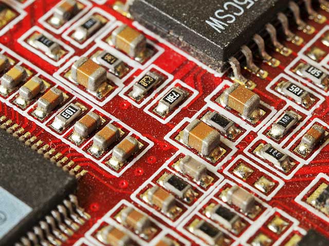
Transistors are switches that control the movement of electrons through material to conduct the electrical currents needed to run circuits, thus enabling logical operations and signal amplification. Field effect transistors (FETs) are a variation of transistors which is used in power electronics including electric cars, but there are many efforts to replace them with more efficient tunneling fiend effect transistors (TFETs).
“The tunneling field effect transistors have not yet demonstrated a sufficiently large drive current to make it a practical replacement for current transistor technology”, said Sean Rommel, associate professor of electrical and microelectronic engineering. “But this work conclusively established the largest tunneling current ever experimentally demonstrated, answering a key question about the viability of tunneling field effect transistor technology.”
Rommel worked with David Pawlik, Brian Romanczyk and Paul Thomas, three graduate students in the microelectronic engineering and microsystems engineering programs at RIT. They performed a fabrication and testing procedure to accurately observe and quantify these current levels. Pawlik developed a process to build and test vertical Esaki tunnel diodes which are smaller than 120 nanometers in diameter.
Esaki tunnel diodes were created back in 1957. Being the first quantum devices, these diodes were used to create a map which shows output tunnel currents for a given set of material systems and parameters.

The process developed at RIT allowed the researchers to measure hundreds of diodes per sample, as well as to experimentally observe currents substantially larger than any previously reported tunneling currents. How much larger? The approach offers a single reference to which they can compare results from micro- to mega-ampere range.
“SEMATECH, RIT and Texas State have made a significant breakthrough in the basic materials for the sub 10 nm node with this work”, said Paul Kirsch, director of Front End Processes at SEMATECH. “The research that was presented at the International Electron Devices Meeting on III-V Esaki tunnel diode performance resolves fundamental questions on the viability of tunneling field effect transistors and provides a practical basis for low-voltage transistor technologies.”
This work is significant because it provides new insight for many research groups focused onto design of higher performance TFETs that could be used in our everyday electronics. The ability to record 2.2 MA/cm2 and 1.1 MA/cm2(-0.3 V), lays the groundwork for III-V TFETs at the 7 nm technology node. In comparison, current top range of computer processors use 22 nm technology.
For more information, you can read the paper named: “Benchmarking and Improving III-V Esaki Diode Performance with a Record 2.2 MA cm2 Current Density to Enhance Tunneling Field-Effect Transistor Drive Current” [366KB PDF].
Share:

-
-
-
-
-
-


Leave your response!