
Data storage – 10 terabits on one coin-size surface
 Imagine all the data which could be stored on 250 DVDs. A team from the University of Massachusetts Amherst and the University of California Berkeley said they had found a faster, more efficient way of making a thin semiconductor film that, by their claims, could dramatically improve data storage.
Many teams have tried to use polymers to create sheets of semiconductor films but the material often lost its structure when spread over large surfaces. To overcome this, the team lead by Thomas Russell of the University of Massachusetts heated sapphire crystals to create a specific pattern of ridges on the surface. This served as a guide for the semiconductor film.
Russell conceived of this new approach with co-lead investigator Ting Xu, a UC Berkeley assistant professor with joint appointments in the Department of Material Sciences and Engineering and the Department of Chemistry. Xu explained that the molecules in the thin film of block copolymers – two or more chemically dissimilar polymer chains linked together – will self-assemble into a precise, equidistant pattern when spread out on a surface. For more than a decade, researchers have been trying to exploit this characteristic for use in semiconductor manufacturing, but they have been constrained because the order starts to break down as the size of the area increases.
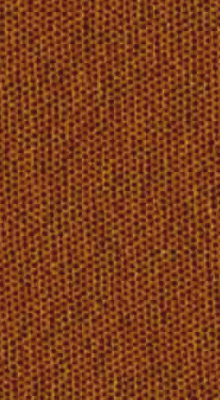
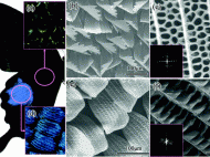
Once the formation breaks down, the individual domains cannot be read or written to, rendering them useless as a form of data storage. To overcome this size constraint, Russell and Xu conceived of the elegantly simple solution of layering the film of block copolymers onto the surface of a commercially available sapphire crystal. When the crystal is cut at an angle – a common procedure known as a miscut – and heated from 1,300 to 1,500 °C for 24 hours, its surface reorganizes into a highly ordered pattern of sawtooth ridges that can then be used to guide the self-assembly of the block polymers.
With this technique, the researchers were able to achieve defect-free arrays of nanoscopic elements with feature sizes as small as 3 nanometers. Because crystals come in a variety of sizes, there are few limitations to how large this block copolymer array can be produced, the researchers said. They also noted that the angle and depth of the sawtooth ridges can be easily varied by changing the temperature at which the crystal is heated to fine tune the desired pattern.

Other research teams are engaged in similar efforts to break the size barrier of self-assembled block copolymers, but this new project by the UMass Amherst-UC Berkeley scientists differs in that it does not rely upon advances in lithography to achieve its goals.
Russell and Xu’s approach differs from how other researchers have been trying to increase storage density. Most have been using optical lithography, which sends light through a mask onto a photosensitive surface. That process creates a pattern to guide the copolymers into assembling.
The new technology could create chip features just 3nm across, outperforming current microprocessor manufacturing techniques, which at their best create features about 45nm across. Photolithography is running into basic barriers to achieving greater density, and the new approach uses less environmentally harmful chemicals, Xu said. But actually applying the technique to CPUs would pose some challenges, such as the need to create random patterns on a CPU, Xu said.
Along with the evolution of media and the development of holograms or environmentally projected images, the hunger for data storage density is growing higher.
In the semiconductor industry, optical lithography is a process in which light passes through a mask with a desired circuit pattern onto a photosensitive material, or photoresist, that undergoes a chemical change. Several steps of chemical treatment are then used to develop the desired pattern for subsequent use. An added benefit, said Xu, is that “our technique is more environmentally friendly than photolithography, which requires the use of harsh chemicals and acids.”


Miniature has become the order of the day.
Data storage – 10 terabits on one coin-size surface –Unimaginable!
This shows the quest of the brain to conquer brain(Memory).
Dr.A.Jagadeesh Nellore (AP), India