
First optoelectronically active 3D photonic crystal developed
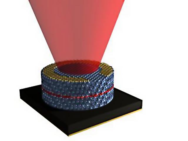 Previous attempts at making 3D photonic crystals have resulted in devices that are only optically active (they can’t turn electricity to light or vice versa). A group of researchers, led by researchers from the University of Illinois, have managed to develop the first optoelectronically active 3D photonic crystal. The development could enable new advancements for solar cells, lasers, metamaterials and more.
“We’ve discovered a way to change the three-dimensional structure of a well-established semiconductor material to enable new optical properties while maintaining its very attractive electrical properties”, said lead researcher Paul Braun, a professor of materials science and engineering and of chemistry at University of Illinois at Urbana-Champaign.
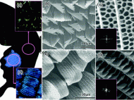
To create a 3D photonic crystal that is both electronically and optically active, the researchers started with a template of tiny spheres packed together. Then, they used gallium arsenide (GaAs) to fill the gaps between the spheres through the template. The GaAs grows as a single crystal from the bottom up in a process called epitaxy.
Epitaxy is common in industry to create flat, two-dimensional films of single-crystal semiconductors, but the researchers developed a way to apply it to an intricate three-dimensional structure. Such approach eliminates many of the defects introduced by top-down fabrication methods, a popular pathway for creating 3-D photonic structures. Another advantage is the ease of creating layered heterostructures.

“The key discovery here was that we grew single-crystal semiconductor through this complex template”, said Braun, who also is affiliated with the Beckman Institute for Advanced Science and Technology and with the Frederick Seitz Materials Research Laboratory at Illinois. “Gallium arsenide wants to grow as a film on the substrate from the bottom up, but it runs into the template and goes around it. It’s almost as though the template is filling up with water. As long as you keep growing GaAs, it keeps filling the template from the bottom up until you reach the top surface.”
Once the template is full, the researchers remove the spheres, leaving a complex, porous 3D structure of single-crystal semiconductor. Then they coat the entire structure with a very thin layer of a semiconductor with a wider bandgap to improve performance and prevent surface recombination.
To test their technique, the group built a 3D photonic crystal LED the first such working device. The LED demonstrates that the concept produces functional devices, but by tweaking the structure or using other semiconductor materials, the researchers believe they can improve solar collection or target specific wavelengths for metamaterials applications or low-threshold lasers.
“With our approach to fabricating photonic crystals, there’s a lot of potential to optimize electronic and optical properties simultaneously”, said Erik Nelson, a former graduate student in Braun’s lab who now is a postdoctoral researcher at Harvard University. “From this point on, it’s a matter of changing the device geometry to achieve whatever properties you want.”
For more information, you can read the article published in the Nature Materials named: “Epitaxial growth of three-dimensionally architectured optoelectronic devices“.


Leave your response!