
Micron’s Hybrid Memory Cube to be produced by IBM
 Memory wall is a term used to describe the greater need for both memory bandwidth and memory density needed for growing number of processor cores in current microprocessors. Whereas DDR4 represents an evolutionary standard, IBM and Micron Technology announced that they will begin production of Hybrid Memory Cube (HMC) – a memory device built using the first commercial CMOS manufacturing technology to employ through-silicon vias (TSVs).
“HMC is a game changer, finally giving architects a flexible memory solution that scales bandwidth while addressing power efficiency”, said Robert Feurle, Vice President of DRAM Marketing for Micron. “Through collaboration with IBM, Micron will provide the industry’s most capable memory offering.”
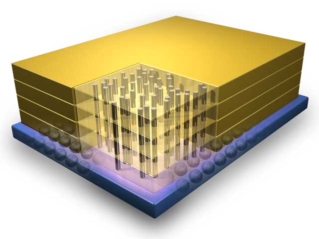
HMC utilizes 3D interconnect technology to blend the best of logic and DRAM processes into a heterogeneous package. At the foundation of HMC is a small high-performance logic layer which sits below vertical stacks of Micron’s DRAM connected by TSV bonds — vertical conduits that electrically connect a stack of individual chips.
An energy optimized DRAM array provides efficient access to memory bits via the logic layer, providing an intelligent memory device truly optimized for performance and energy efficiencies. This elemental change in how memory is built into a system is paramount. By placing intelligent memory on the same substrate as the processing unit, each part of the system can do what it’s designed to do far more optimally than any previous technology. HMC requires 70 percent less energy to transfer data while offering a small form factor — just 10 percent of the footprint of conventional memory.
A single HMC can provide more than 15x the performance of a DDR3 module. Speed is increased by the very fast, innovative interface, unlike the slower parallel interface used in current DRAM modules. Compared to other known current state-of-the-art devices, HMC delivers 10 times higher bandwidth and reaches 128 gigabytes per second (GB/s). With a significant amount of responders built into HMC, its developers expect it to perform with lower queue delays and higher bank availability, which can provide a substantial system latency reduction.
“This is a milestone in the industry move to 3D semiconductor manufacturing”, said Subu Iyer, IBM Fellow. “The manufacturing process we are rolling out will have applications beyond memory, enabling other industry segments as well. In the next few years, 3D chip technology will make its way into consumer products, and we can expect to see drastic improvements in battery life and functionality of devices.”
Hybrid Memory Cube technology could lead to a new generation memory capable to follow growing demands of large-scale networking and high-performance computing. Two months ago, Samsung and Micron started a Hybrid Memory Cube Consortium, and IBM stepped in with their advanced semiconductor fab in East Fishkill, N.Y., where they will use the company’s 32nm, high-K metal gate process technology to produce HMCs.


Finally, a memory that can follow Moore’s law. I doubt it will reach consumer market anytime soon due to its price.
I wouldn’t be too sure about your claim RS, many great minds made a similar mistake in recent past when they spoke about technology.
If this technology becomes established, the initial price could soon be well worth the improvement in performance.