
Two methods to produce graphene nanoribbons
 You remember we wrote about carbon nanotubes (CNTs) in one of our previous articles? Two groups of researchers have found ways to unfold CNTs in order to make nanoribbons of graphene. The experts claim that the development could point the way towards a new generation of electronics, including computer chips that are faster and tinier than the silicon-based chips used today.
Graphene, an atom-thick sheet of honeycombed carbon, is one of the hottest materials around. It conducts electrons well, but is thin, transparent and strong, making it potentially useful in displays and solar panels. Ribbons of graphene could be more useful still. At widths of around 10 nanometers or less, electrons are forced to move lengthwise, and make the graphene behave as a semiconductor.
However, the ribbons have proved extremely difficult to produce. In previously used methods nanoribbons of graphene were cut from larger sheets using chemical methods that, like a blunt pair of scissors, offer little control over the width of the ribbons. In the two new studies the research groups found ways to unroll carbon nanotubes to produce nanoribbons.
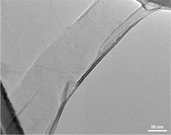
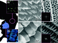
One team, led by the Hongjie Dai from the Stanford University, is making graphene nanoribbons (GNRs) – materials with properties distinct from those of other carbon allotropes. The all-semi-conducting nature of GNRs could bypass the problem of the extreme chirality dependence of the metal or semiconductor nature of CNTs in future electronics. Currently, making GNRs using lithographic chemical or sonochemical methods is challenging. It is difficult to obtain GNRs with smooth edges and controllable widths at high yields. The making of GNRs is done by fixing nanotubes onto a polymer film and then using ionized argon gas to cut away a strip of each tube.
Once cleaned, the GNRs have smooth edges and a narrow width distribution (10–20nm). Raman spectroscopy and electrical transport measurements reveal the high quality of the GNRs. Unzipping CNTs with well-defined structures in an array will allow the production of GNRs with controlled widths, edge structures, placement and alignment in a scalable fashion for device integration.

The other team, led by the James Tour from the Rice University lab, has uncovered a room-temperature chemical process that splits CNTs in order to make flat nanoribbons. The technique makes it possible to produce the ultra thin ribbons in bulk quantities. These ribbons are straight-edged sheets of graphene, the single-layer form of common graphite found in pencils. You’d have to place thousands of them side by side to equal the width of a human hair, but tests show graphene is 200 times stronger than steel.
The process involves sulfuric acid and potassium permanganate. The chemical reacts with single and multi-walled carbon nanotubes and unzips them in a straight line. The unzipping action can start on the end or in the middle, but the result is the same – the tubes turn into flat, straight-edged, water-soluble ribbons of graphene. When produced in bulk, these microscopic sheets can be “painted” onto a surface or combined with a polymer to let it conduct electricity. The resulting ribbons are wider (around 100–500 nm) and aren’t semi-conducting, but are easier to make in large quantities.
Nearly all of the nanotubes subjected to unzipping turn into graphene ribbons, Tour said, and the basic process is the same for single or multi-walled tubes. Single-walled carbon nanotubes convert to sheets at room temperature and are good for small electronic devices because the width of the unzipped sheet is highly controllable. But the multi-walled nanotubes are much cheaper starting materials and the resulting nanoribbons would be useful in a host of applications.
The researchers say there are an enormous number of potential applications for nanoribbons. Tour’s larger ribbons could be used in touch-screen displays, flexible electronics, and solar panels, he says, noting that his nanoribbons are easy to process because they are graphene oxide, which is soluble in water. Dai’s thinner ribbons are more likely to be used in electronics due to their semi-conducting ability and smaller size. The researchers say that the methods are being licensed for commercial development.


Leave your response!