
Extreme Ultraviolet (EUV) lithography makes 13.5 nm circuits
 Microchips and integrated circuits in today’s computers and devices are becoming increasingly smaller and more complex. If you ever followed news about components or read vanity bragging from device manufacturers, you may have noticed they use terms concerting circuit printing technology or lithography. Fraunhofer Institute researchers claim they have found the next generation solution that could be used for mass-production of smallest circuits thus far.
While newest Intel Ivy bridge processors have reached 22 nm lithography, a multidisciplinary team of researchers from the Fraunhofer Institute (FI) came up with extreme ultraviolet (EUV) radiation lithography – a process which employs light with wavelengths in the EUV range to print dense 13.5 nm circuits.
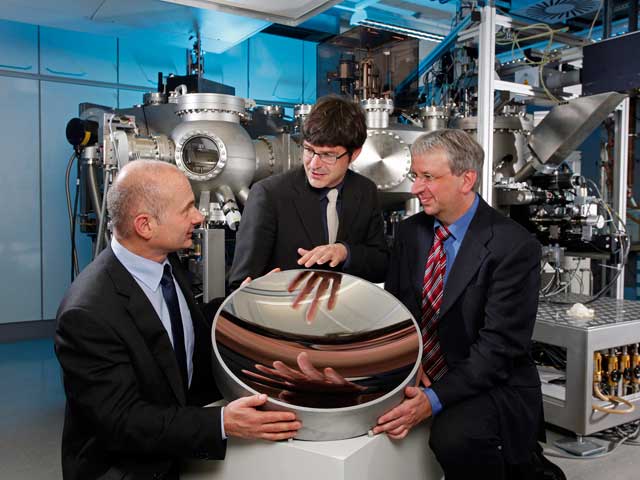
Led by Dr. Klaus Bergmann from the FI for Laser Technology (ILT) Aachen, Dr. Stefan Braun the FI for Material and Beam Technology (IWS) Dresden, and Dr. Torsten Feigl from the FI for Applied Optics and Precision Engineering (IOF) Jena, their teams have developed key elements for EUV lithography:
- light sources (developed by ILT)
- collector optics (developed by IOF)
- illumination and projection optics (developed by IWS)
Efficiency of the light source is the key to the industrial use of EUV. ILT team developed the first prototypes of the EUV source as early as 2006, and the latest model is based on the rapid, pulsed discharge of electrically stored energy. In the process, a small amount of tin is vaporized using a laser and excited with a high current to an emission at 13.5 nm.
“The challenge we faced was to develop and apply a multilayer coating system that combined high EUV reflectance with high thermal and radiation stability onto the strongly curved collector surface”, said Torsten Feigl from IOF.
The quality of the collector mirror is crucial to the radiation hitting the exposure mask in exactly the right place. The coating guarantees that the losses remain low and that the quality of the focused EUV radiation is high. IOF team managed to develop the world‘s largest multi-layer coated EUV mirror with a diameter of more than 660 millimeters.
Once the radiation passed the mask, it is exposed onto the chips via further projection mirrors. IWS team came up with the optimum reflection layer for these components. Magnetron sputtering ensures maximum layer accuracy, without additional polishing processes or direct thickness control being required. One machine type for large area precision coating is already in industrial use.
As pioneers of the EUV radiation lithography, researchers from Fraunhofer Institute managed to establish themselves as key partners for the supplier industry both in and outside Europe, and we could expect the new lithography technology to be used in industrial production by 2015.


Congratulations to colleagues, combined with other manufacturing techniques this could be the winner along with X-ray radiation lithography.