Geckos biomimicry used for new method in electronics printing
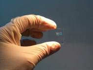
 Inspired by geckos, a team of engineers has developed a reversible adhesion method for printing electronics on a variety of tricky surfaces such as clothes, plastic and leather. Researchers from Northwestern University and the University of Illinois at Urbana-Champaign designed a square polymer stamp that allows them to vary its adhesion strength. The stamp can easily pick up an array of electronic devices from a silicon surface and move and print them on a curved surface.
“Our work proposes a very robust method to transfer and print electronics on complex surfaces”, said Yonggang Huang, Joseph Cummings Professor of Civil and Environmental Engineering and Mechanical Engineering at Northwestern’s McCormick School of Engineering and Applied Science. Huang led the theory and design work at Northwestern, while his colleague John Rogers, the Flory-Founder Chair Professor of Materials Science and Engineering at the University of Illinois, led the experimental and fabrication work.
Four pyramid-shaped tips on the stamp’s bottom are located at each corner of square and squeezable polymer stamps. They mimic the micro- and nano-filaments on the gecko’s foot, which the animal uses to control adhesion by increasing or decreasing contact area with a surface.
Pressing the stamp against the electronics causes the soft tips to collapse up against the stamp’s body, maximizing the contact area between the stamp and the electronics and creating adhesion. The electronics are picked up in a complete batch, and, with the force removed, the soft tips snap back to their original shape. The electronics now are held in place by just the four tips, a small contact area. This allows the electronics to be easily transferred to a new surface.
“Design of the pyramid tips is very important”, Huang said. “The tips have to be the right height. If the tips are too large, they can’t pick up the target, and if the tips are too small, they won’t bounce back to their shape.”
The researchers conducted tests of the stamp and found the changes in contact area allow the stamp’s adhesion strength to vary by 1,000 times. They also demonstrated their method can print layers of electronics, enabling the development of a variety of complex devices. For more information read the PNAS paper named: “Microstructured Elastomeric Surfaces with Reversible Adhesion and Examples of Their Use in Deterministic Assembly by Transfer Printing”.


Excellent.
Dr.A.Jagadeesh,Nellore(AP),India