
Harvard researchers use nanoFETs to delicately probe cells
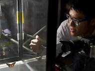
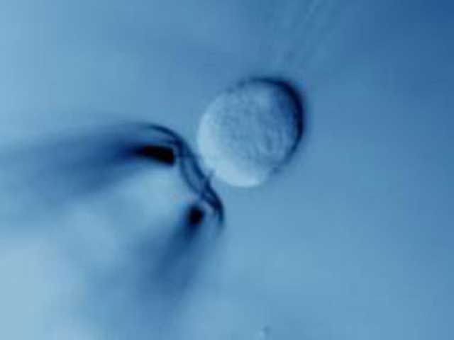 Chemists and engineers at Harvard University have used nanowires in order to make a new type of V-shaped transistor small enough to be used for sensitive probing of the interior of cells. The new device is smaller than many viruses and about one-hundredth the width of the probes which are currently used to take cellular measurements and potentially damage cells upon insertion, thus reducing the accuracy or reliability of any data gained.
“Our use of these nanoscale field-effect transistors, or nanoFETs, represents the first totally new approach to intracellular studies in decades, as well as the first measurement of the inside of a cell with a semiconductor device”, says senior author Charles M. Lieber, the Mark Hyman Jr. Professor of Chemistry at Harvard. “The nanoFETs are the first new electrical measurement tool for intracellular studies since the 1960s, during which time electronics have advanced considerably.”
Lieber and colleagues say nanoFETs could be used to measure ion flux or electrical signals in cells, particularly neurons. The devices could also be fitted with receptors or ligands to probe for the presence of individual biochemicals within a cell.
Human cells can range in size from about 10 microns (millionths of a meter) for nerve cells to 50 microns for cardiac cells. While current probes measure up to 5 microns in diameter, nanoFETs have less than 50 nanometers in total size, with the nanowire probe itself measuring just 15 nanometers in diameter. Lieber and his team found that by coating the structures with a phospholipid bilayer (the same material cell membranes are made of) the devices are easily pulled into a cell via membrane fusion.

“This eliminates the need to push the nanoFETs into a cell, since they are essentially fused with the cell membrane by the cell’s own machinery”, Lieber says. “This also means insertion of nanoFETs is not nearly as traumatic to the cell as current electrical probes. We found that nanoFETs can be inserted and removed from a cell multiple times without any discernible damage to the cell. We can even use them to measure continuously as the device enters and exits the cell.”
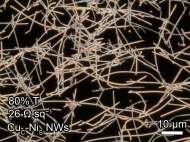
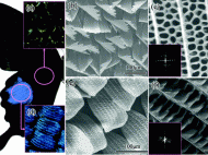
This research builds upon previous work by Lieber’s group to introduce triangular “stereocenters” (fixed 120-degree joints) into nanowires, structures that had previously been rigidly linear. These stereocenters, analogous to the chemical hubs found in many complex organic molecules, introduce kinks into 1-D nanostructures, transforming them into more complex forms.
Lieber and his co-authors found that introducing two 120-degree angles into a nanowire in the proper cis orientation creates a single V-shaped 60-degree angle, perfect for a two-pronged nanoFET with a sensor at the tip of the V. The two arms can then be connected to wires to create a current through the nanoscale transistor.


Leave your response!